I will start working with the PSoC Creator IDE and the PSoC 4 BLE Pioneer Kit (CY8CKIT-042-BLE-A) . I will not start with the blinking LED or any of the tutorials that are explained on the Cypress website. You can find the intro videos through their website or on YouTube. I will dig into the meat of things right away. So to start with the fun stuff let's get the LCD working. As I mentioned in the previous post I have a 1.44" LCD with the ILI9163 driver. To understand what is needed to interface let's look at the details of the board. Let's first look at the board we have and the pin configuration.

As you can see in the image we have the following pin connections:
- LED
- SCK
- SDA
- A0
- RESET
- CS
- GND
- VCC
Now we need to determine how to connect these pins to our Pioneer Kit to start working with the LCD. We can always use a bit banging method, but for this case we will use the built in SPI functions. According to the PSoC 4XX8 BLE 4.2 Family Datasheet there are two SCB (Serial Communication Blocks) that can be used. These support I2C, UART, or SPI interfaces. In our case one of the two SCB's will use the SPI interface to interface with the LCD. With these we have a few different options for pins to choose (see Table 4. Port Pin Connections from the datasheet). The options are as follows:

For this project I have chosen the following pins to use for the SPI communications:
| PSoC Board | LCD | Desciption |
| P1[4] | SDA | SPI Data (MOSI) |
| P1[6] | CS | Chip/Slave Select |
| P1[7] | SCK | SPI Clock |
*Note: The datasheet shows the pin reference with a period for example P1.4. Once we get to the IDE you will see the pins are referenced using brackets, for example P1[4]. For the remaining parts of this blog I will match what is shown in the IDE.
So you are probably wondering what about the fourth pin. Each section shows four pins and I only show three. For the LCD I have chosen there is no pin for the MISO (Master In Slave Out). What this means is there is only one way communication. From the master device (PSoC) to the slave device (LCD). So now we have three of the eight pins for the LCD assigned, but what do we do for the remaining. Below shows the other pins I will use to interface with the LCD. You can find more information on the Pioneer Kit at the this link (CY8CKIT-042-BLE-A Bluetooth Low Energy Pioneer Kit Guide).
| PSoC Board | LCD | Desciption |
| V3.3 | LED | LED Backlight |
| V3.3 | VCC | LCD Power |
| GND | GND | LCD Ground |
| P1[0] | A0 | Data/Command |
| P1[1] | RESET | Reset pin |

For now I will connect these pins to the LCD through a breadboard and some jumper wires. This will help give me something to physically work with an prototype. Now that have the connections made
I can open up the PSoC Creator IDE and start on the software side.
Open up the PSoC Creator IDE and create a new blank project. We will walk through adding piece by piece. For me I drew a block to represent the LCD and connections so I could easily reference it. Then I show the connections to the different pins/blocks. The image below shows what I created in the IDE TopDesign.cysch. It is not required but for me I can easily reference this for my connections.

I am going to start with the easier part which are the two pins outside of the SPI block. They are labeled LCD_DC and LCD_Reset. To create these you can drag the Digital Output Pin (found under the Ports and Pins) to the schematic.

Once this is dragged in we can double click on the symbol in the schematic or right click and go to "Configure". Once you do this a window will open up. There are three sections we will need to update.
- Name - Pick a name of the pin that makes sense to you (I chose LCD_Reset)
- HW connection - Uncheck this as we will not connect this to another block in the schematic.
- Initial drive state - Make this Low(0). This is the initial state of the pin on power up.
Once you have this configure, go ahead and press the "OK" button at the bottom the window.

Now I will configure the other pin call LCD_DC. See the screenshot below.

Before I define the pins these are connected to I will move on to another block that needs to be configured. This is the SCB for the SPI communications to the LCD. Under the component catalog tree find the "Communications" section, then find the "SPI" section and you should find a component labeled SPI (SCB mode). There will be a version number listed after that which may or may not match depending on your version of IDE. See image below for the communication block that was added to my schematic.

Once we have this added go ahead and open up the configuration. If it is not already on the "Configuration" tab go ahead and click this. You should have the radio button marked for SPI and feel free to rename to what you would like. This name will be used in the API's when we start the coding so don't make it too complex.

Once you have finished with the "Configuration" tab block on the "SPI Basic" tab. This is where it get's a little complicated if you are not familiar with SPI communications. I will not go through all of this but you should understand SPI communications when configuring. Here is a link to the Wikipdia site for SPI Communications. For our case we are using 8-bit transmission and the SPI mode = 0 (CPHA = 0 & CPOL = 0). The chip select (or slave select) is active low which means when you pull this pin low the slave is active. Then recall from before that this is a 3-wire SPI communications so we do not require the MISO pin connection. Most of this information can be taken from the ILI9163 datasheet. Along with this I needed to understand the PCB I have that came with the LCD. Looking at the datasheet you can see there are several models such as SPI & parallel that can be configured for this driver chip. It does take time to put the pieces together but this is where you do learn quite a bit of information. It does get easier the more datasheets you review as well.

The last tab we will review is the "SPI Adavanced" tab. In this tab you should not need to configure anything but I will review quickly in case there are some differences. I have the buffer size set to 8 and no interrupts selected. As we get things working we may review this tab including the DMA portion. Using the DMA could help take some of the load off of the microcontroller if needed. For now we will keep it as is.

Wow, a lot of information just to get the schematic portion going. In other microcontrollers you would need to configure a lot of this in code and review the datasheet of the microcontroller to understand how to configure. We will get to the code portion, but next we need to configure the pins for the blocks we just entered in the schematic.
To get to the pin configurations in the "workspace explorer" section (by default on the left) double click on the "Pins" section under Design Wide Resources. On the right hand side you need to configure the pins for the blocks we entered under the schematic. For now we have the following five pins to configure.
- P1[4] SPI Data (MOSI)
- P1[6] SPI Chip/Slave Select
- P1[7] SPI Clock
- P1[0] Data/Command
- P1[1] Reset pin

Once you have the pins configured go ahead and build the project so the API's can be built and we can start working with the API's. You can press SHIFT+F6, right click on the project and select BUILD from the pull down menu or use the toolbar on top and go to the "Build" tab and select Build XYZ where XYZ is the name of your project. If this is successful you should get a note that states "Build Succeeded: xx/yy/zz hh:mm:ss". If you have made it this far you are ready to start the coding portion.

Now let's open up the main.c file located under Source Files. As you can see this is built with some code already populated. There is a #include "project.h". If you go to this file you will see it has been populated based on the items we populated in the schematic. This provides the references to the API's that we will be using. There is also a line of code:
CyGlobalIntEnable;
We will keep this line of code in for future use of interrupts.

So to interface with the LCD there are a few functions we need to write. One is the transmission of data through the SPI interface. This allows us to send data (or commands) to the LCD through the SPI interface. I have set up a function that sends an 8-bit value then a separate one that will send a 16-bit value (essentially splits the 16-bit value into two 8-bit values). I also have a function called lcd_init. This initializes and configures the LCD which is required before sending any data. I have also created another function called lcd_setScreen which will set the entire LCD to the color defined.
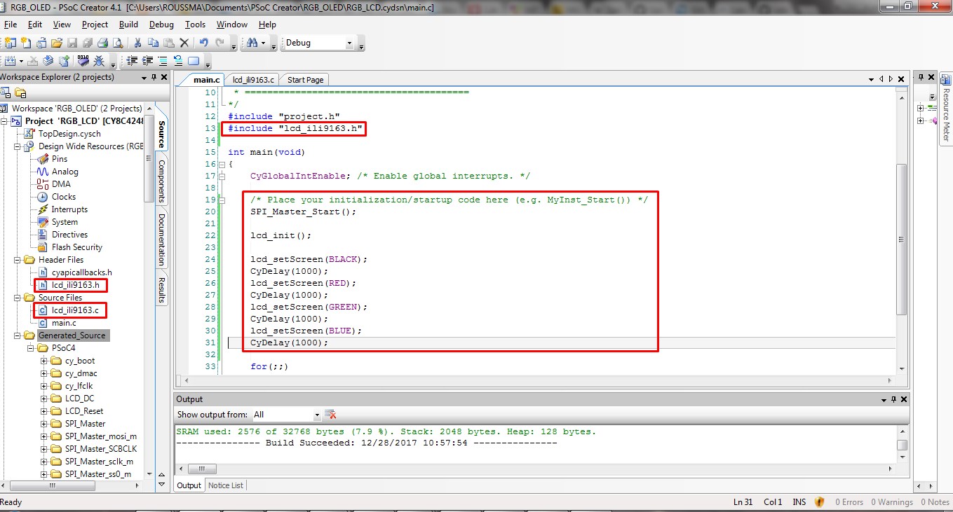
So as seen in the image below to make all of this work you need to add the .c and .h file that has been created for the LCD (ili9163) to the project. Next you need to include the lcd_ili9163.h file in the main.c. Then after the main loop we will do the following:
- Start the SPI communications
- Initialize the LCD
- Set the screen to BLACK
- Delay 1 second
- Set the screen to RED
- Delay 1 second
- Set the screen to GREEN
- Delay 1 second
- Set the screen to BLUE
- Delay 1 second
- Enter the continuous for loop (where we do nothing)
I have uploaded the files on my Github account which can be found at the following link:
In the next blog I will add on to the existing LCD capabilities including the ability to display text and images.

